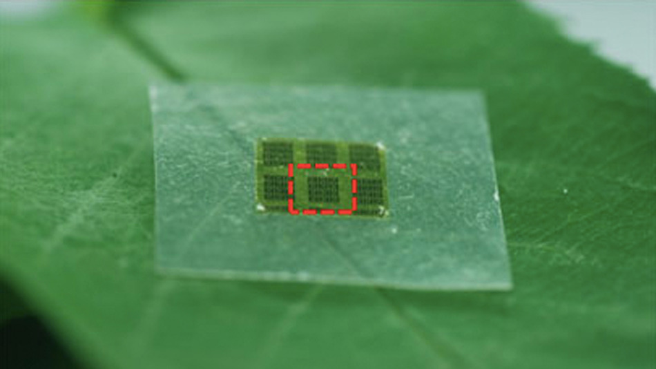
Biodegradable, wood-based computer chips can perform just as well as chips commonly used for wireless communication, according to new research.
The inventors argue that the new chips could help address the global problem of rapidly accumulating electronic waste, some of which contains potentially toxic materials. The results also show that a transparent, wood-derived material called nanocellulose paper is an attractive alternative to plastic as a surface for flexible electronics.
In conventional chip manufacturing, electronic components like transistors are made on the surface of a rigid wafer made of a semiconducting material such as silicon. Researchers at the University of Wisconsin, led by Zhenqiang (Jack) Ma, a professor of electrical and computer engineering, made the electronic components in a similar way but then used a rubber stamp to lift them from the wafer and transfer them to a new surface made of nanocellulose. This reduced the amount of semiconducting material used by a factor of up to 5,000, without sacrificing performance.
In two recent demonstrations, Ma and his colleagues showed they can use nanocellulose as the support layer for radio frequency circuits that perform comparably to those commonly used in smartphones and tablets. They also showed that these chips can be broken down by a common fungus. these chips can be broken down by a common fungus.
The vast majority of the semiconducting material in today's chips makes up the support layer, and the active electronic components represent only a very tiny fraction. This is an expensive waste, says Ma, and in the case of some materials it can lead to dangerous pollution when a device is thrown out.
In recent years, researchers have demonstrated that nanocellulose, which is made by breaking wood fibers down to the nanoscale, can be a viable support material for a variety of electronic devices, including solar cells. However, the recent demonstrations are the first to reveal properties that make the material promising for use in efficient, high-performing radio frequency circuits, says Ma.
Ma says chips like those his group made are ready for commercialization. But he thinks it's likely to take heightened environmental pressure, or a spike in the price of rare semiconductor materials like gallium, for the mainstream electronics industry to change its current practices and consider making chips from wood.
Techniques for manufacturing devices like those Ma and his colleagues have made are becoming more established in the electronics industry Techniques for manufacturing devices like those Ma and his colleagues have made are becoming more established in the electronics industry, says John Rogers, a professor of materials science at the University of Illinois at Urbana-Champaign. Rogers originally developed the method Ma's group used to transfer small amounts of semiconducting material from a large wafer to the nanocellulose surface.
The military is very interested in "transient electronics" that would degrade in some way to prevent sensitive electronics from falling into the hands of adversaries, says Rogers. But perhaps the most important aspect of Ma's recent demonstrations is the potential environmental benefit, he says. Devices of all shapes and sizes that can communicate wirelessly are proliferating quickly, and this trend shows no signs of slowing. People upgrade their devices often, and outdated devices are commonly thrown out. "What's happening to all those waste streams? I think that's a pretty legitimate question to ask," he says.
Fuente: mashable.com